
Dr. Wataru Nakagawa's Lab
Design, build and characterize optical nanostructures for interdisciplinary applications
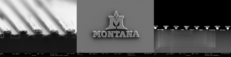
Subwavelength scale (<1 micron) structures can have interesting and useful optical properties, as the interaction of light with such small structures can be very different from larger structures. Recently, it has become possible to manufacture structures on this size scale by borrowing fabrication technologies from the semiconductor industry. These engineered optical devices (sometimes called “meta-materials”) have a broad range of applications including advanced imaging, remote sensing, optical communications and integrated photonic systems.
Effective use of nanoscale optical phenomena to produce functional optical devices requires expertise and innovation in a number of areas:
- Accurate electromagnetic modeling tools for nanostructure design and simulation
- Optimization of nanofabrication techniques for device fabrication
- Precision optical measurement tools for device characterization
- Interdisciplinary applications (in collaboration with other research groups at MSU and worldwide)
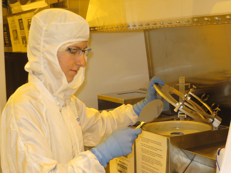
The Nano Optics group works in all of the above areas to advance new optical devices from concept to application. In most cases, undergraduate research assistants will focus on one or two of the above areas.
The Nano Optics Group is looking for motivated students to assist with our work in
the design, manufacturing, and testing of these devices. Current work focuses on nanostructures
with polarization selectivity for applications in LIDAR and atmospheric science. Some
background in optics, electromagnetics, or microfabrication (clean room processing)
is preferable, but not required. All research students are expected to be motivated,
hard-working, detail-oriented, creative problem solvers, and ready to learn!

 logo")